R&D and Engineering
Mechanical, electrical and firmware engineering from requirement to approved prototype.
Engineering starts from a written specification, not from a picture of a similar product. Before any CAD work the requirement is reduced to the three numbers that decide most of a beauty device: the target landed cost, the certification route for the destination market, and the size of housing someone is willing to hold for ten minutes.
Those constraints usually conflict. A slimmer housing means a smaller battery and shorter runtime; a cheaper MCU means fewer functions or a slower sensor read; a larger battery can move the product into a different transport classification. We put the trade-off in writing and let the buyer choose, instead of choosing quietly and meeting the problem again at tooling.
How a project runs
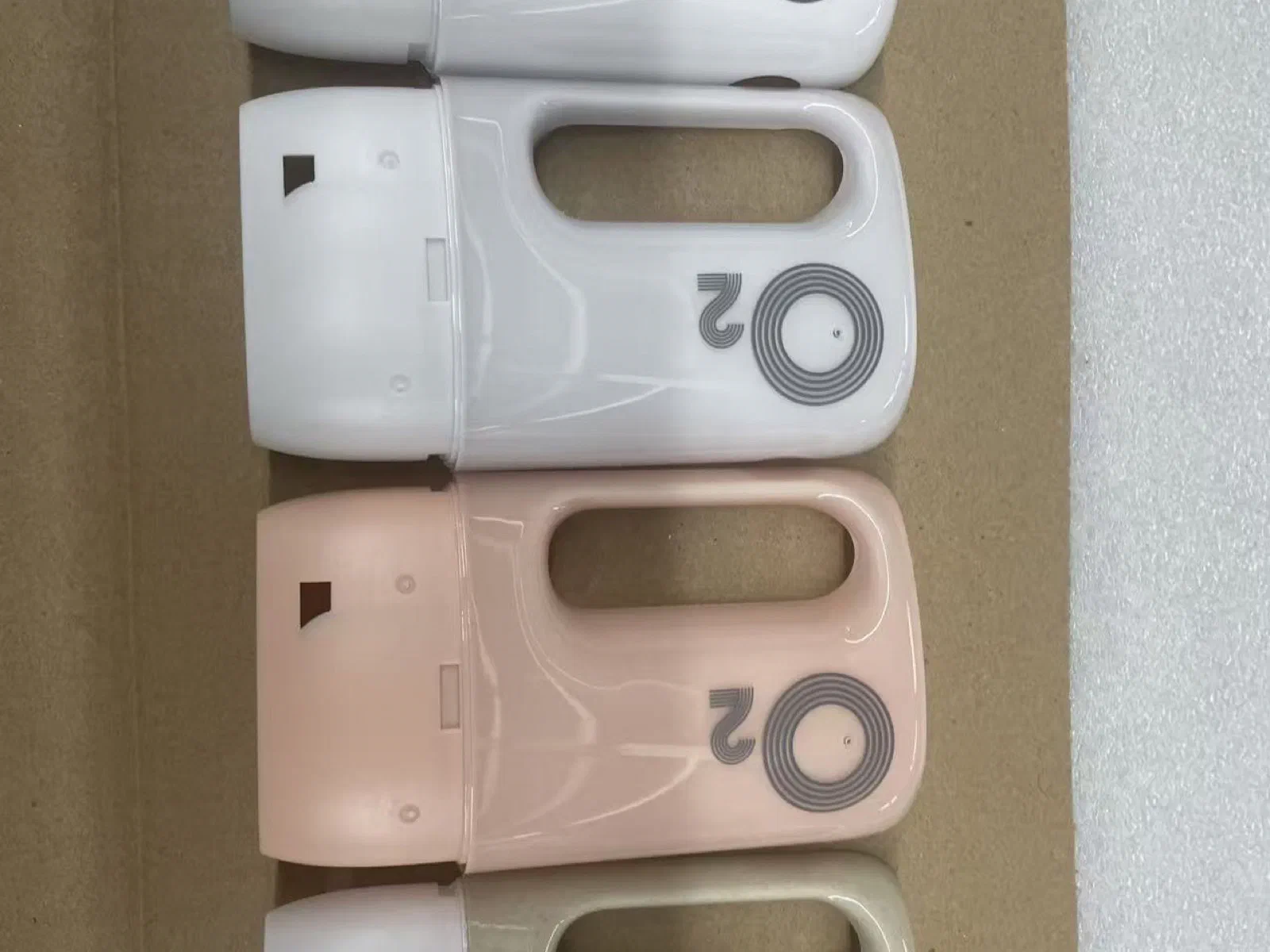
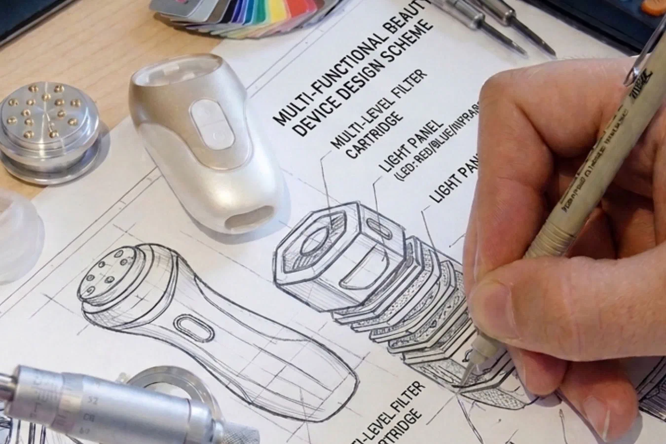
A development cycle moves through requirement, concept, mechanical design, electronics, prototype and validation. Prototypes are built on 3D-printed and CNC parts first, so fit and feel can be judged before steel is cut. The functional sample then runs on the production PCBA, so firmware is tested against the electronics it will actually ship with.
Validation carries most of the risk. A device that works on the bench can still fail on drop, on temperature cycling, or after a hundred charge cycles. We test the prototype against the same criteria the production unit will face, and report what failed rather than only what passed.
Why the electronics stay in-house
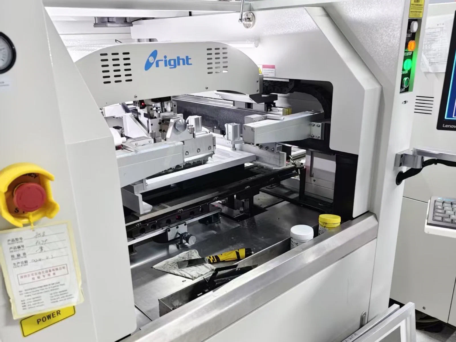
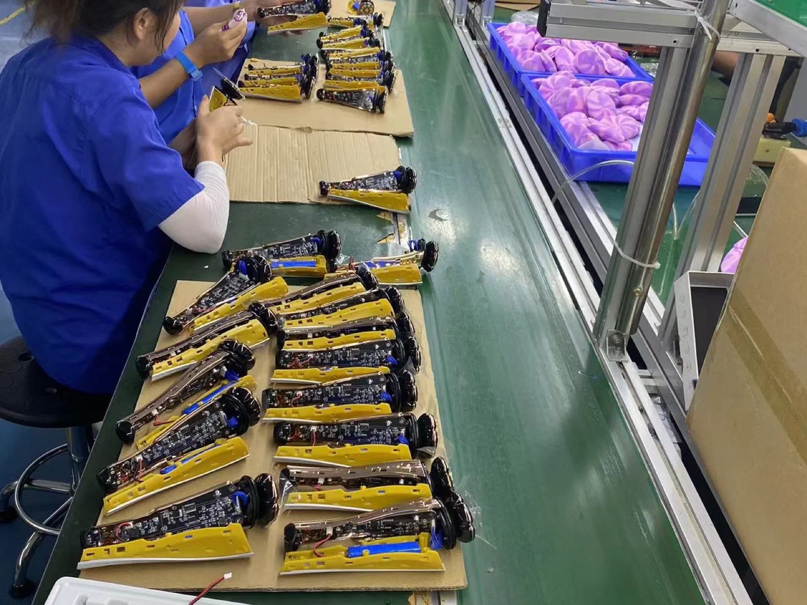
Control boards are designed and placed in the same building as the housing. When a layout has to change — a component goes end-of-life, an EMC margin is too thin, a supplier raises a price — there is no external queue to wait in.
At a glance
- Engineering disciplines
- Mechanical structure, electronics, firmware and test — all in-house
- Engineers
- 50 across mechanical, electronics, firmware and quality
- Prototype route
- 3D print and CNC for fit and feel first, then a functional sample on the production PCBA
- Sample lead time
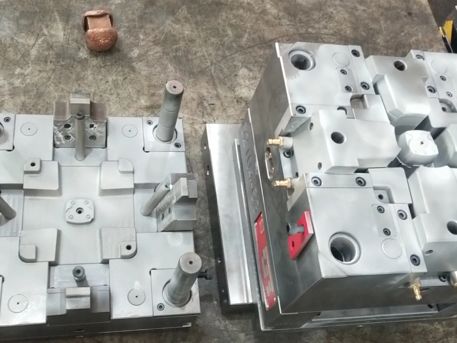
- 7 days on an existing platform; longer when a new mold is required
- Handover package
- 3D files, 2D drawings, schematic, BOM, firmware and a test plan
What you get